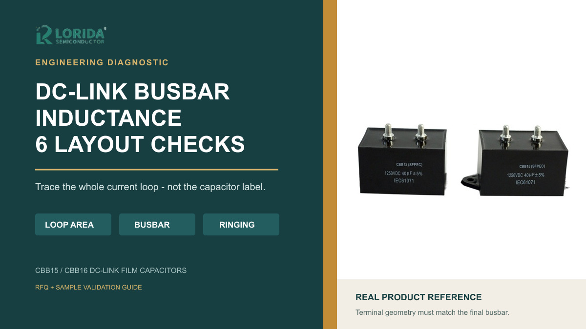
DC-link busbar inductance must be evaluated as one assembled current loop, because the capacitor, terminals, busbar, power module, spacing and mutual coupling interact. A low-ESL capacitor can still produce excessive switching overshoot or ringing when the connection loop is long, asymmetric or poorly coupled. For a traceable RFQ, send the final busbar drawing, switching edge information, current spectrum, terminal geometry and measurement method, then validate the assembled loop in the real converter.
Key Takeaways
What engineering and procurement should freeze
Evaluate the capacitor and busbar as an interacting loop, not as isolated ESL values.
Keep positive and negative current paths close, broad and symmetric where the system design allows.
Attach frequency, temperature and measurement conditions to every current, ESR and ESL value.
Require the exact terminal pattern, busbar stack and power-module location in the sample drawing.
Validate overshoot, ringing and temperature in the final mechanical assembly before approval.
Why the assembled loop controls switching stress
Individual inductance values do not simply add
Fast current changes create voltage across stray inductance according to the relationship V = L × di/dt. The useful design value is therefore the inductance of the complete commutation loop. TDK’s 2026 practical-use white paper gives a concrete example in which component contributions were characterized as 3.1 nH, 3.7 nH and 1.1 nH. Their arithmetic sum was 7.9 nH, while the measured or characterized total assembly was 8.3 nH because electromagnetic interaction changed the result. These figures describe TDK’s example only, but they demonstrate why adding catalogue numbers is not a valid system proof.
Wide-bandgap switching raises the layout penalty
SiC and other fast-switching power stages can operate with steep current edges. A larger loop area or an unnecessary terminal extension can translate that edge into higher overshoot, ringing and electromagnetic stress. TDK’s B25696H announcement illustrates the conditions attached to one modern DC-link series: 47 µF to 1,280 µF, 900 VDC to 2,000 VDC, self-inductance as low as 30 nH and ESR down to 0.8 mΩ at 10 kHz. Those are TDK-series values, not LORIDA specifications. Their procurement lesson is that capacitance, voltage, ESL, ESR, frequency and construction must stay tied to one exact order code.
Six diagnostic checks for the busbar layout
Normalize every proposal with one comparison table
| Check | Evidence required | Failure signal |
|---|---|---|
| 1. Current loop | Marked commutation path on the assembly drawing | Long or separated return path |
| 2. Terminal pattern | Exact pitch, polarity and contact geometry | Forced bends or uneven current sharing |
| 3. Busbar stack | Layer order, thickness, overlap and insulation | Large loop area or local neck-down |
| 4. Symmetry | Parallel-path geometry and current distribution | One winding or terminal runs hotter |
| 5. Measurement | Probe loop, bandwidth and switching condition | Unrepeatable overshoot or ringing |
| 6. Thermal result | Case, terminal and hotspot method | Acceptable voltage but excessive heating |
1. Trace the complete commutation loop
Mark the path from the capacitor’s positive terminal through the switching device and back to the negative terminal. Include terminal extensions, laminated-busbar transitions, bolted joints, PCB copper and power-module connections. The drawing should show dimensions and layer relationships, not only a simplified schematic. If several capacitors operate in parallel, show how each unit joins the shared path and identify any unequal path length.
2. Match the exact terminal interface
The sample must use the production terminal pitch, contact surface, hole or thread, polarity and mounting orientation. A substitute case can change current spreading even when its capacitance and rated voltage match. TDK’s February 2026 xEVCap assembly note explains that a single unit may not meet the capacitance, RMS current, ESL or power needs of a typical 150 to 300 kW traction inverter, so modular assemblies and their busbar interfaces must be evaluated together. That power range belongs to TDK’s application context, not to a LORIDA product rating.
3. Minimize loop area without creating a bottleneck
Overlapping positive and negative conductors can reduce the external magnetic field and loop inductance, but the complete stack still needs adequate creepage, clearance, insulation and current capacity. Review narrow bridges, abrupt turns, spacer blocks and fastener clearances. A wide busbar that necks down at the capacitor terminal can concentrate current and heat. Record conductor material, thickness, plating, contact preparation and the insulating layer in the controlled drawing.
4. Check current sharing in parallel assemblies
Parallel capacitors do not automatically share ripple current equally. Small differences in path impedance, terminal position and mutual coupling can move current toward one branch. Compare path length and geometry, then measure terminal or case temperature for every unit at representative load. TDK’s B25696H announcement links homogeneous current distribution to its internal busbar configuration and reports ripple-current capability up to 91 A at 60 °C ambient and 10 kHz for that series. Keep all three conditions attached to the value; do not copy 91 A into another design.
5. Measure overshoot and ringing with a controlled probe
Probe technique can create or hide the symptom. State the probe type, bandwidth, ground or differential connection, measurement points, load current, DC-bus voltage, gate resistance, switching speed and temperature. Use the same setup when comparing revisions. Record both peak overshoot and ringing frequency, then correlate the waveform with the physical loop change. Do not approve a layout from one unexplained screenshot.
6. Close the electrical and thermal gates together
Reduced ringing does not prove acceptable temperature, and acceptable case temperature does not prove adequate switching margin. Measure the capacitor case, terminals and nearby busbar at worst-case operating states. Ask the supplier how internal hotspot and life are estimated for the exact series. Vishay’s MKP1848C data sheet, for example, lists a 105 °C maximum permissible case temperature with voltage derating and a useful-life estimate above 100,000 hours at rated voltage and 70 °C for that series. These are conditional manufacturer values, not universal limits.
Frequently Asked Questions
Can a low-ESL capacitor fix an inductive busbar?
No. A low-ESL capacitor helps, but the assembled loop still determines the result. Terminal extensions, busbar separation, power-module position, joints and mutual coupling can dominate or alter the total inductance. Request the exact capacitor and mechanical drawing, model the complete loop, and validate overshoot with a controlled probe in the production geometry. If the capacitor is changed without revising the busbar, record whether terminal pitch, contact area and loop path also changed. Catalogue ESL is a component condition, not an automatic system-level guarantee.
What should be included in a DC-link busbar RFQ?
Send the electrical mission profile and the dimensioned mechanical stack together. Include nominal and maximum DC voltage, current spectrum, switching frequency and edge information, capacitance target, ambient and cooling conditions, power-module location, positive and negative busbar layers, insulation, terminal geometry, mounting, creepage and clearance constraints. Ask for the exact series, controlled drawing, ESR and ESL conditions, permitted ripple current, thermal method and sample-validation plan. Freeze the final capacitor, busbar revision and measurement setup in the approval record.
How should two layout revisions be compared?
Compare them with the same capacitor, load state, switching settings, probe setup and temperature condition. Photograph the assembly and mark the current loop for each revision. Record peak overshoot, ringing frequency, settling behavior, capacitor and terminal temperatures, busbar temperature and any current-sharing evidence. If gate resistance or switching speed changes, treat it as a separate experiment because it alters di/dt. A layout revision is ready only when its electrical, thermal, insulation and mechanical checks pass together.
Build a traceable sample plan
Link the drawing, waveform and approved part number
Start with LORIDA’s DC-link capacitor selection page and the CBB15/CBB16 product category. For the wider thermal boundary, review the DC-link thermal validation guide. When the controlled drawing and operating profile are ready, send them through the LORIDA contact page for exact-series discussion. Final suitability remains subject to the current data sheet and real-assembly validation.
Primary sources
Verified references for exact data
Send the busbar drawing, switching conditions and waveform evidence with the capacitor RFQ.
Last Updated: November 18, 2026. Third-party numerical examples are cited engineering references and are not blanket LORIDA product specifications. Verify the exact order code, controlled drawing and final equipment requirements before approval.